Rigid Flex in RF/Microwave
Rigid flex combines the best features of rigid and flexible circuit boards to offer users a robust, high-performance design. This hybrid type of PCB is ideal for applications that require a combination of reliability, strength and flexibility, such as medical imaging equipment, military missile guidance systems and industrial machinery. Rigid flex can also be used in consumer electronics, like wearable devices and automotive infotainment systems.
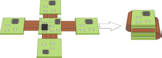
In rigid flex, the conductor paths of rigid areas are connected by flexible sections that can be bent or twisted without disrupting electrical performance. This allows the PCB to be shaped into 3-dimensional structures, providing spatial degrees of freedom that address space and weight concerns. It eliminates the need for interconnecting hardware and reduces overall product weight.
This hybrid circuit board design is well suited for use in environments that experience vibration, shock and other environmental stresses. Its hybrid construction provides improved mechanical stability, reducing the risk of fatigue or cracking in these harsh conditions. Additionally, the ultra-thin nature of flex circuit materials and the ability to create narrow circuit traces makes for higher connection density and reduced overall system weight.
Rigid Flex in RF/Microwave Applications
Rigid flex can be produced using several different fabrication methods, including the tape or open cavity method and the cocoon or closed cavity method. The latter is preferable as it provides a more streamlined process, requiring less cleaning steps and allowing for faster production. Both techniques are effective in protecting the flex materials during plasma, electroless copper and copper plating processes.
It can be challenging to design a rigid flex, but with the help of experienced engineers and specialized software, this can be accomplished. In addition to choosing the right FR-4 or other rigid flex materials, it’s important to take into account the thickness of the copper and the amount of adhesive used on the traces. The recommended minimum bend radius is 10 times the material thickness for single-sided flex and 20 times for multilayer flex, while it’s essential to avoid right angles where possible.
Once the PCB has been designed, the manufacturing process can begin. To ensure the rigid and flex areas remain aligned, it’s vital to follow IPC-2223 design guidelines when routing and placing components. This helps to prevent signal reflections, reduce copper waste and optimize traces for the bending environment. It’s also recommended to use a thicker adhesive than the copper, and avoid any plated holes or vias within 100 mils of any rigid-flex interface.
The rigid-flex PCB is a cost-effective, reliable solution for any application that requires a combination of strength and flexibility. It also offers the added benefit of reducing assembly time, as it eliminates the need for additional connectors and wire harnesses between rigid components. This helps to streamline the assembly process and makes for a more streamlined and aesthetically pleasing device. It’s also easier to test the rigid flex unit prior to installation, making it a good option for long-production runs of complex electronic products.